Programming and debugging connectors can consume a surprising amount of PCB area, particularly on compact embedded products where board space and enclosure height are tightly constrained.
A conventional 10-way SWD header adds both PCB footprint and Z-height, while alternative approaches such as edge connectors or device-specific test clips can introduce restrictions on PCB layout or target hardware.
This project explores a compact spring-loaded programming clip that connects directly to exposed SWD pads on the target PCB. The aim is to remove the permanent programming connector from the product while retaining a reliable, reusable interface for firmware development, production programming and debugging.
Key Technical Responsibilities
Compact Target Interface: Developed a six-via SWD footprint requiring no permanent programming connector on the target PCB.
Low Z-Height: Eliminated programming-header height from the finished product.
Flexible PCB Placement: Designed the interface so the programming connection is not restricted to a board edge.
Mechanical Location & Retention: Used rounded pogo-pin tips locating into through-hole vias to provide both electrical contact and mechanical registration of the programming clip.
Electrical Validation: Verified SWD programming and debugging through repeated firmware programming tests.
Design for Manufacture: Developed the mechanical components around fabrication methods suitable for prototyping and potential low-volume production.
Reusable Platform: Designed the clip around the standard SWD interface rather than a specific MCU package.
Solution Research
Several common programming approaches were reviewed before developing the clip.
A conventional 1.27 mm 10-way SWD header is simple and reliable but occupies valuable PCB area and remains permanently fitted to the target hardware. Edge-mounted programming contacts remove the connector but constrain placement to the perimeter of the PCB, while MCU-specific test clips provide limited portability between designs.
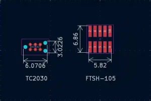
Commercial pogo-pin interfaces such as the Tag-Connect TC2030 provide an effective alternative and significantly reduce connector overhead. However, their mechanical retention features and associated keep-out requirements still consume useful board space.
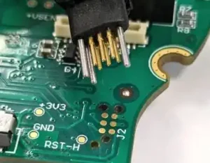
The concept developed here instead uses a compact array of six plated through-hole vias as the programming interface. Rounded spring-loaded pogo-pin tips partially locate into the vias when the clip is fitted. This provides electrical contact while also helping to locate and mechanically retain the clip against the PCB.
As a result, no dedicated programming connector or additional locating holes are required on the finished product. Only the six SWD vias remain on the target PCB, and these can be positioned away from the board edge where the surrounding layout allows.
This approach is particularly suited to compact embedded products where PCB area, enclosure height or component placement make a conventional programming header undesirable.
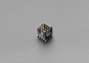
Standard FTSH-105 1.27mm pitch 10-way SWD debugging header.TC2030Surface area comparison TC2030 VS FTSH-105.
Mechanical Design
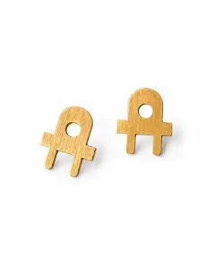
Minion Pins – Laser-cut brass hinge components
The clamping mechanism is a fully custom design developed specifically for the programming clip. Several hinge concepts were sketched and evaluated before settling on a compact arrangement that could be manufactured inexpensively and integrated directly into the FR4 clip body.
The hinge components are laser-cut from thin brass sheet. Brass was selected for its low cost, good machinability and, importantly, excellent solderability. This allows the hinge components to be soldered directly onto the FR4 structure, avoiding additional brackets, fasteners or machined assemblies.
The small hinge plates were informally nicknamed “minion pins” during development due to their distinctive shape.
The V1.0 mechanism successfully demonstrates the basic clamping concept, but testing identified an opportunity to increase and better control the contact force applied to the pogo pins. A torsion spring is therefore planned for the V2.0 design, providing a more positive closing force and improving the consistency of electrical contact with the target PCB.
This approach keeps both part count and fabrication cost low while leaving considerable scope to refine the mechanical behaviour in the next revision.
Testing & Qualification Stage
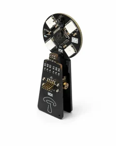
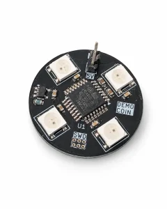
DemoCoin – demonstration PCB for the SWD clip V1.0.
A dedicated test PCB, nicknamed the DemoCoin, was designed to validate the programming clip independently of other projects.
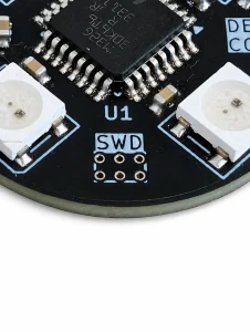
The board incorporates an STM32 microcontroller, status LEDs and a six-via SWD interface matching the pogo-pin arrangement of the clip.
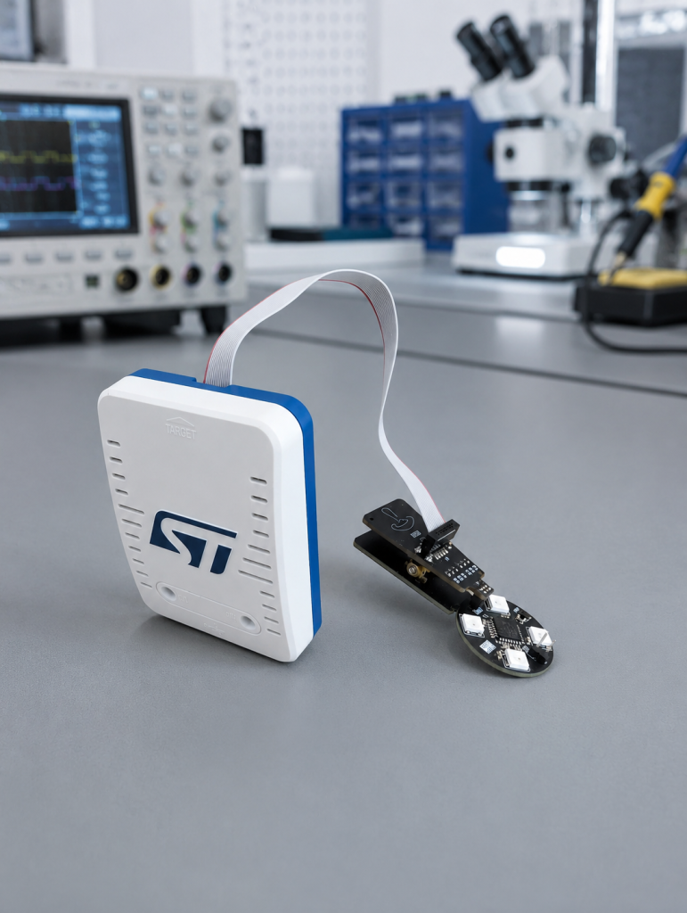
Repeated programming and debugging tests were carried out using the V1.0 prototype and a standard ST-Link interface. Multiple firmware builds were successfully programmed and executed through the clip, demonstrating reliable electrical connection when correctly fitted.
The testing also validated the basic mechanical principle. The rounded pogo-pin tips locate into the through-hole vias, helping the clip remain aligned and attached during programming without requiring a conventional connector or separate locating features.
Practical use of V1.0 has nevertheless identified opportunities to improve the overall mechanism, particularly the ease of attachment and consistency of pogo-pin engagement. These findings will inform the future V2.0 revision.
SWD programming clip target contact area
Conclusion & Engineering Retrospective
The V1.0 prototype has successfully demonstrated the core concept: reliable SWD access can be achieved using a compact array of through-hole vias rather than fitting a permanent programming connector to the target PCB.
A particularly effective aspect of the design is the interaction between the rounded pogo pins and the target vias. The pins partially locate into the holes, so the electrical interface also contributes to mechanical alignment and retention. This keeps the PCB-side interface extremely simple.
Development of V1.0 also showed that the main opportunities for improvement are mechanical. While the underlying contact principle works, the next revision will focus on making attachment easier and improving the consistency with which all pogo pins engage the target simultaneously.
These changes have not yet been designed or manufactured and will form the basis of a future V2.0 prototype. With the electrical interface already proven, the next development stage can concentrate on usability, repeatability and manufacturability before considering a small production run.