Location: Brisbane, QLD

24-Bit ADC Product Cost Reduction & Optimisation

Professional Project
Project Type B2B Consulting
Hardware Status V2.0
Organisation Spark Product Solutions
Completion Date 2026 - Present

Problem Outline

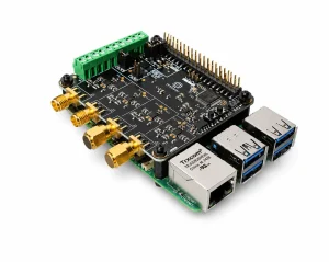
SPS-PI-ADC1 high-precision 24-bit ADC HAT+.

The client had an existing Revision 1 high-precision ADC product which had already entered low-volume production and gained initial customers. The next stage of development was to reduce manufacturing cost and improve design efficiency without unnecessarily redesigning a proven product.

The SPS-PI-ADC1 is a four-channel, 24-bit Delta-Sigma ADC HAT+ designed for precision data acquisition using the Raspberry Pi platform. The product combines simultaneous analogue capture, configurable active filtering, deterministic sampling and a low-noise analogue signal chain within a compact stackable module.

The engineering brief was therefore focused on targeted optimisation: review the existing design and BOM, identify meaningful cost-saving opportunities, simplify circuitry where practical and establish measured baseline performance before progressing to a Revision 2 PCB.

Key Technical Responsibilities

  • BOM Cost Reduction: Reviewed the complete production BOM and identified component substitutions and design changes achieving a reduction of just over 20% in BOM cost at low-volume build quantities.
  • Circuit Optimisation: Redesigned the precision ADC reference-voltage circuitry, reducing a three-IC implementation to a single-device solution.
  • Component Rationalisation: Reduced unique BOM line items by standardising passive component values and package sizes where electrically and mechanically appropriate.
  • Component Sourcing: Investigated lower-cost alternatives for high-value components including SMA connectors, board connectors, ICs and user-interface switches.
  • Performance Characterisation: Developed and executed noise-performance testing to establish a measured baseline for the existing Revision 1 hardware.
  • Test Automation: Developed Python scripts to automate measurement capture, storage and processing of large ADC datasets.
  • Technical Documentation: Authored the draft technical product datasheet covering product architecture, interfaces, analogue filtering, specifications and measured performance.
  • Client Liaison: Worked directly with the client throughout the redesign to review proposed changes and maintain alignment with product and commercial requirements.

BOM Cost Reduction & Component Rationalisation

As the product was already being manufactured and supplied to customers, the objective was not to redesign every component purely for minimum cost. Instead, the BOM review concentrated effort where it would provide a meaningful commercial return while minimising unnecessary engineering and requalification work.

Particular attention was given to relatively high-value components including the SMA connectors, general-purpose connectors, integrated circuits and tactile switches. Suitable lower-cost alternatives were identified where the electrical, mechanical and availability requirements could be maintained.

The passive component population was also reviewed to reduce unnecessary BOM complexity. Where appropriate, common resistor and capacitor values and package sizes were reused across the design rather than maintaining functionally unnecessary variants. Less common resistance values could also be formed using combinations of existing standard values where this reduced the number of unique purchased parts without compromising circuit performance.

Combined with the circuit-level changes, this review achieved a BOM cost reduction of just over 20% for low-volume production builds.

ADC Reference Circuit Simplification

Review of the analogue circuitry identified a further opportunity within the ADC reference-voltage generation.

The Revision 1 design used a precision voltage-reference IC followed by two operational-amplifier stages configured as a composite reference buffer. While electrically capable, the arrangement increased component count, board area and BOM cost.

The reference architecture was reviewed and redesigned around a simpler single-IC solution capable of providing the required precision reference function without the additional buffer devices.

This change reduced the reference section from three ICs to one, simultaneously reducing component cost, BOM line count and circuit complexity.

The revised circuit forms part of the Revision 2 schematic and will be validated on the next hardware build.

Noise Performance Characterisation

Before modifying the analogue design, baseline noise performance of the existing Revision 1 hardware was characterised to provide an objective reference against which future revisions could be evaluated.

A Python-based test workflow was developed to automate data acquisition and analysis. For the documented noise test, the analogue input was connected to analogue ground and 12,000 ADC measurements were captured and processed to determine RMS noise, peak-to-peak noise, effective resolution and noise-free resolution.

The resulting dataset established a measured baseline of approximately 38.3 µV RMS noise, with a noise-free resolution of approximately 16 bits under the documented test conditions.

Automating the measurement and analysis process provided a repeatable method that can be reused when Revision 2 hardware becomes available, allowing the impact of the cost-down and circuit changes to be assessed directly against the original product.

Product Documentation:

Alongside the hardware development, a new technical datasheet was produced to better document the capabilities and architecture of the product.

The document covers the ADC architecture, Raspberry Pi interface, modular stacking arrangement, configurable analogue filtering, electrical and mechanical specifications, measured noise performance and typical application scenarios.

Producing the documentation alongside the engineering review also provided an opportunity to consolidate technical information about the existing product and establish a clearer reference for future customers and subsequent hardware revisions.

Current Status:

The Revision 2 schematic changes have been completed and the updated PCB is currently progressing through layout.

The next hardware revision incorporates the cost-reduction and circuit-simplification work described above. Once manufactured, the revised hardware can be characterised using the same automated noise-performance test methodology established on the Revision 1 boards, allowing direct comparison of the two designs.

Engineering Retrospective

This project demonstrates a different type of product-development challenge from designing new hardware from a blank sheet.

Because the Revision 1 product was already functional and in the hands of customers, the objective was to identify changes that offered worthwhile commercial benefit without introducing unnecessary redesign risk.

The most effective savings did not come solely from searching for cheaper equivalents component by component. Reviewing the architecture itself identified opportunities such as simplifying the ADC reference circuitry, while component rationalisation reduced both unit cost and purchasing complexity.

For a relatively low-volume product, this targeted approach provided a practical balance between engineering effort, manufacturing cost and technical risk. The resulting Revision 2 design reduces BOM cost by more than 20% while retaining the fundamental architecture and functionality of the established product.

Scroll to Top